PM Modi Lays Foundation for South India’s First Semiconductor Packaging Plant
PM Modi laid the foundation stone for ASIP Technologies’ INR 2,387 crore semiconductor packaging facility in Visakhapatnam.
You're reading Entrepreneur India, an international franchise of Entrepreneur Media.
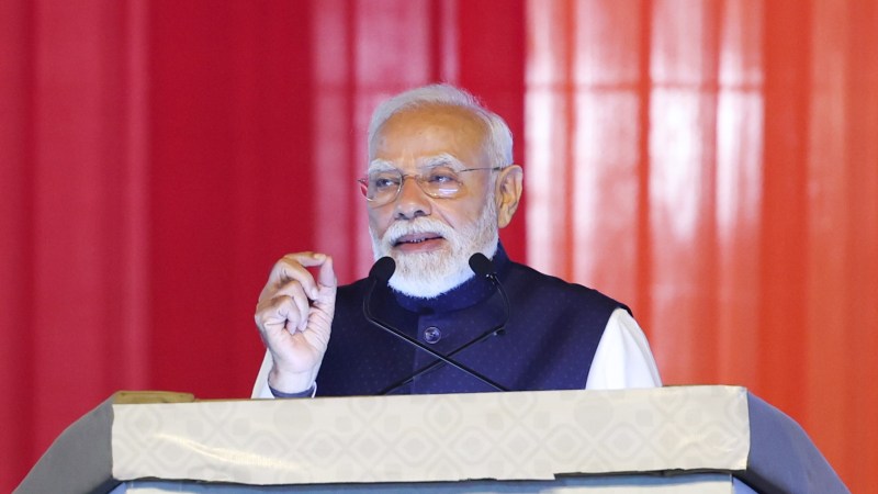
Prime Minister Narendra Modi laid the foundation stone for ASIP Technologies’ INR 2,387 crore semiconductor packaging facility in Visakhapatnam, marking the launch of South India’s first semiconductor plant approved under the India Semiconductor Mission (ISM). The project is expected to strengthen India’s semiconductor manufacturing capabilities and support the country’s push towards self-reliance in chip production.
Located at Tarluvada in Visakhapatnam, the unit will focus on semiconductor packaging and testing. It is designed to cater to applications across sectors including automotive, telecommunications, consumer electronics, industrial systems and AI.
This project is among the semiconductor facilities approved under the India Semiconductor Mission, the Centre’s flagship programme aimed at building a domestic semiconductor ecosystem spanning chip design, manufacturing, assembly and packaging. The Andhra Pradesh facility is expected to strengthen the country’s semiconductor supply chain while generating skilled employment in the region.
The foundation stone was laid during a programme in which the Prime Minister inaugurated and launched development projects worth nearly INR 18,000 crore across Andhra Pradesh, covering sectors such as infrastructure, transport and aviation.
Prime Minister Narendra Modi laid the foundation stone for ASIP Technologies’ INR 2,387 crore semiconductor packaging facility in Visakhapatnam, marking the launch of South India’s first semiconductor plant approved under the India Semiconductor Mission (ISM). The project is expected to strengthen India’s semiconductor manufacturing capabilities and support the country’s push towards self-reliance in chip production.
Located at Tarluvada in Visakhapatnam, the unit will focus on semiconductor packaging and testing. It is designed to cater to applications across sectors including automotive, telecommunications, consumer electronics, industrial systems and AI.
This project is among the semiconductor facilities approved under the India Semiconductor Mission, the Centre’s flagship programme aimed at building a domestic semiconductor ecosystem spanning chip design, manufacturing, assembly and packaging. The Andhra Pradesh facility is expected to strengthen the country’s semiconductor supply chain while generating skilled employment in the region.
The foundation stone was laid during a programme in which the Prime Minister inaugurated and launched development projects worth nearly INR 18,000 crore across Andhra Pradesh, covering sectors such as infrastructure, transport and aviation.